Subject: Physics | Level: A-Level | Exam Board: AQA
AQA Option F Electronics demands a rigorous synthesis of analogue signal processing via operational amplifiers and digital logic systems, including sequential circuits. You will design functional subsystems, derive component values mathematically, and apply circuit theory to real-world problems — skills that examiners test with multi-step calculations, circuit design tasks, and Boolean minimisation. Master this topic and you unlock some of the most reliably mark-rich questions on the A-Level paper.
Revision Notes & Key Concepts
Revision Podcast Transcript
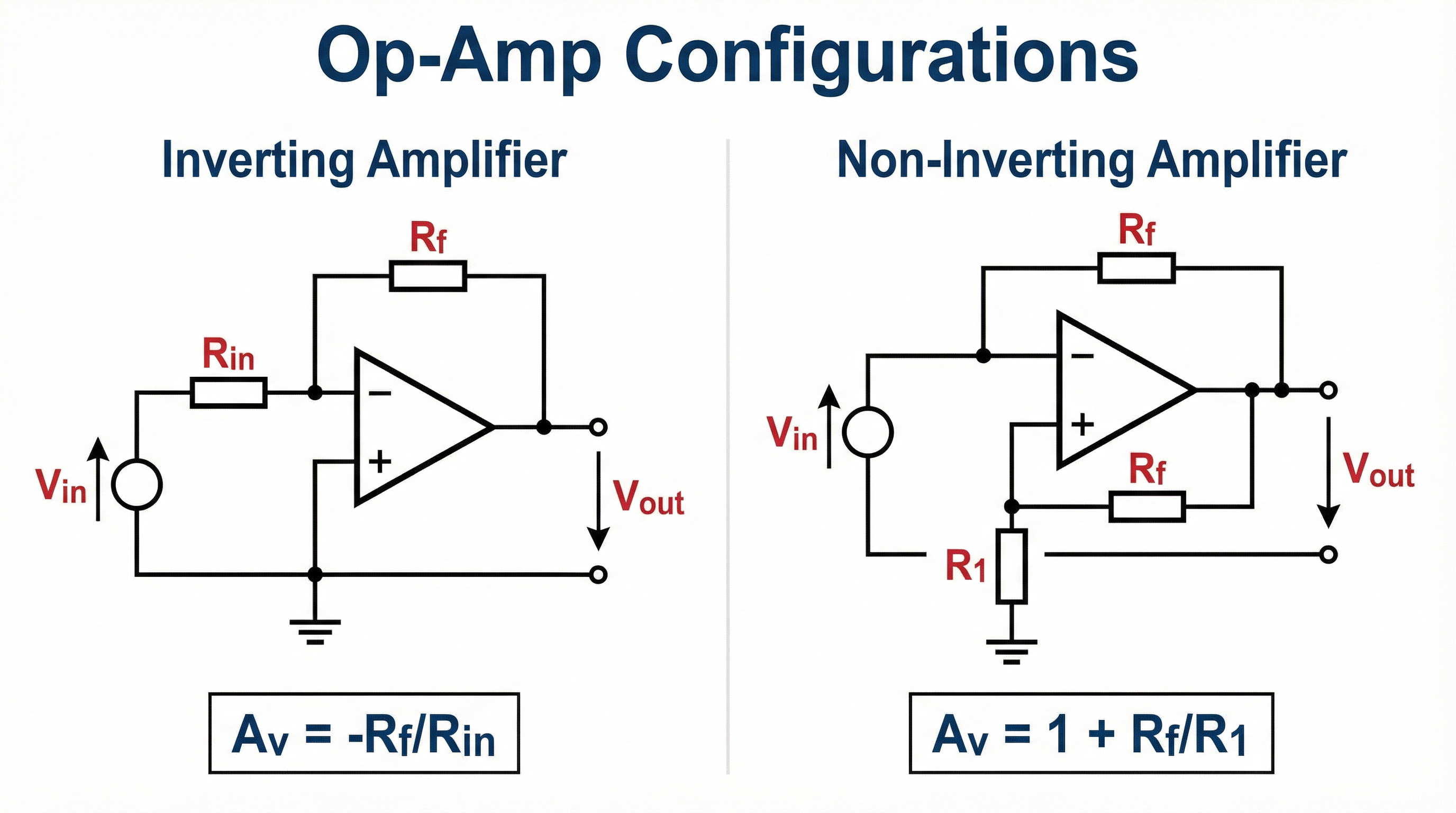
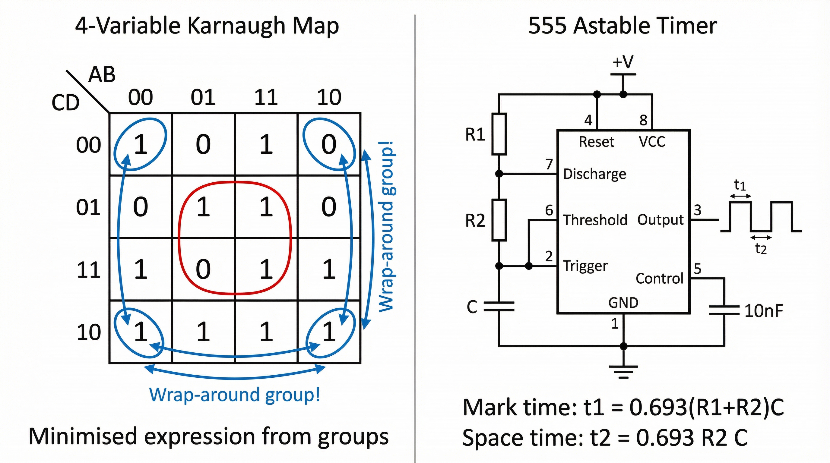
AQA A-Level Physics: Electronics — Study Podcast Approximate duration: 10 minutes Voice: Female, warm, conversational, enthusiastic tutor --- INTRO (approx. 1 minute) --- Hello and welcome! I'm really glad you've hit play on this one, because today we're diving into one of the most rewarding — and honestly, one of the most satisfying — topics in AQA A-Level Physics Option F: Electronics. I'm talking about operational amplifiers, digital logic, Karnaugh maps, the 555 timer, and signal processing. These topics sit at the intersection of physics and engineering, and once they click, they really click. Whether you're revising for your first sitting or pushing for that A-star, this podcast is going to walk you through the core concepts clearly, flag the exact mistakes that cost candidates marks every year, run you through a quick-fire quiz, and leave you with a sharp summary to carry into the exam hall. So grab a pen, get comfortable, and let's get into it. --- CORE CONCEPTS (approx. 5 minutes) --- Let's start with the operational amplifier — the op-amp. Think of it as the Swiss Army knife of analogue electronics. It's a high-gain differential amplifier: it amplifies the difference between two input voltages. The key properties of an ideal op-amp are infinite open-loop gain, infinite input impedance, and zero output impedance. In real life, these aren't quite true — but for AQA exam purposes, you treat the op-amp as ideal unless the question specifically tells you otherwise. Now, there are two configurations you absolutely must know. First: the inverting amplifier. The input signal goes through a resistor called R-in to the inverting, or minus, input. A feedback resistor R-f connects the output back to that same inverting input. The non-inverting plus input is connected to ground. The voltage gain formula is: A-v equals minus R-f divided by R-in. That negative sign is critical — it tells you the output is 180 degrees out of phase with the input. Candidates lose marks every year by forgetting that negative sign. Don't be one of them. Second: the non-inverting amplifier. Here, the input goes directly to the non-inverting plus input. The gain formula is: A-v equals 1 plus R-f divided by R-1. Notice it's always greater than 1, and there's no phase inversion. Here's a crucial point that examiners love to test: saturation. The output voltage of an op-amp cannot exceed the supply rail voltage. So if your gain calculation gives you, say, minus 15 volts, but the supply rails are plus and minus 12 volts, the actual output is saturated at minus 12 volts. You must state this explicitly. The mark scheme says: 'credit calculation of voltage gain only if the final answer explicitly acknowledges saturation limits imposed by the supply rails.' So always check your calculated output against the supply voltage. Now let's talk about filters. Op-amps are used to build active filters — circuits that pass certain frequencies and block others. A low-pass filter passes low frequencies and attenuates high ones. A high-pass filter does the opposite. The break frequency — also called the cut-off frequency — is given by: f equals 1 divided by 2 pi R C. At this frequency, the gain drops to 70.7 percent of its maximum, which is minus 3 decibels. Make sure you identify which R and which C are responsible for the cut-off — examiners want you to be specific. Moving on to digital electronics. The foundation here is Boolean algebra and logic gates. You need to know AND, OR, NOT, NAND, NOR, and XOR gates, their truth tables, and their Boolean expressions. De Morgan's Laws are essential for simplification. The first law says: NOT of A AND B equals NOT-A OR NOT-B. The second law says: NOT of A OR B equals NOT-A AND NOT-B. These let you convert between NAND and NOR implementations, which is a common exam task. Karnaugh maps — K-maps — are your tool for minimising Boolean expressions. The golden rules are: group only 1s, groups must be powers of 2 (so 1, 2, 4, 8, or 16 cells), make groups as large as possible, and — this is the one candidates miss — groups can wrap around the edges and corners of the map. Those wrap-around groups are called 'wrapping groups,' and failing to spot them leads to non-minimal expressions. The examiner's mark scheme specifically awards marks for correctly identifying wrapping groups. Now, sequential logic. Unlike combinational logic where the output depends only on current inputs, sequential circuits have memory — the output depends on both current inputs and previous states. The D-type flip-flop is the key component here. On the rising edge of a clock pulse, the output Q takes the value of the data input D. This is how registers and counters are built. Finally, the 555 timer in astable mode. This is a circuit that produces a continuous square wave output — it oscillates between high and low without any external trigger. The timing formulas are: the mark time — that's the time the output is high — equals 0.693 times the quantity R1 plus R2 times C. The space time — the time the output is low — equals 0.693 times R2 times C. The total period is the sum of these two, and the frequency is 1 divided by the period. The most common mistake is using R1 plus R2 for the space time instead of just R2. The capacitor charges through both R1 and R2, but discharges only through R2. Keep that distinction sharp. --- EXAM TIPS AND COMMON MISTAKES (approx. 2 minutes) --- Right, let's talk exam technique. This is where marks are won and lost. Tip one: always check for saturation. After calculating your output voltage, compare it to the supply rails. If it exceeds them, state clearly that the output saturates at the supply rail voltage. This is a guaranteed mark. Tip two: the negative sign in inverting amplifiers. Every year, candidates write the gain as positive when it should be negative. The negative sign isn't optional — it tells you about phase inversion, which is a physical property of the circuit. Tip three: Karnaugh map wrapping. Before you finalise your K-map groupings, scan all four edges and all four corners for possible wrap-around groups. A group of four in the corners of a 4-variable K-map is a classic exam trap. Tip four: 555 timer — know which resistor does what. R1 plus R2 for charging, R2 only for discharging. Write this on your formula sheet in the exam. Tip five: command words matter. If the question says 'calculate,' show every step of your working, write the formula first, substitute values, and include units. If it says 'explain,' use the word 'because' to link cause and effect — that's what earns the explanation mark. Tip six: NAND-only or NOR-only implementations. If the question specifies NAND-only logic, every gate in your answer must be a NAND gate. Apply De Morgan's Laws to convert AND and OR gates. Read the question carefully before drawing anything. Tip seven: bandwidth of AM signals. The bandwidth equals twice the highest modulating frequency — not the carrier frequency. This trips up a lot of candidates. --- QUICK-FIRE RECALL QUIZ (approx. 1 minute) --- Okay, quick-fire quiz time. I'll ask the question, give you three seconds to think, then give the answer. Question one: What is the voltage gain formula for an inverting amplifier? ... Answer: A-v equals minus R-f divided by R-in. Question two: What happens to the output of an op-amp if the calculated voltage exceeds the supply rails? ... Answer: The output saturates at the supply rail voltage. Question three: In a 555 astable timer, which resistors does the capacitor charge through? ... Answer: Both R1 and R2. Question four: What is the cut-off frequency formula for an RC filter? ... Answer: f equals 1 divided by 2 pi R C. Question five: State De Morgan's first law. ... Answer: NOT of A AND B equals NOT-A OR NOT-B. How did you do? If any of those caught you out, go back and re-read that section of your notes. --- SUMMARY AND SIGN-OFF (approx. 1 minute) --- Let's wrap up with the five things you absolutely must take into the exam. One: Op-amp gain formulas — inverting is minus R-f over R-in, non-inverting is 1 plus R-f over R-1. The negative sign matters. Two: Always check for saturation — if calculated output exceeds supply rails, state the output saturates. Three: K-map wrapping groups — always check edges and corners before finalising your minimised expression. Four: 555 timer — mark time uses R1 plus R2, space time uses R2 only. Five: De Morgan's Laws — essential for NAND-only and NOR-only circuit conversions. You've got this. Electronics is one of those topics where careful, methodical working really pays off. Show your steps, check your signs, and always read what the question is actually asking. Good luck in your exam — I'm rooting for you. See you in the next episode!
Key Terms & Definitions
- Open-loop gain
- The intrinsic voltage gain of an operational amplifier in the absence of any external feedback network; for an ideal op-amp this is infinite, and for real devices is typically 10⁵ to 10⁶.
- Virtual earth
- The condition at the inverting input of an ideal inverting amplifier where the voltage is maintained at approximately 0 V due to negative feedback, even though it is not directly connected to ground.
- Saturation
- The condition in which the output voltage of an op-amp reaches and is limited by the supply rail voltage (±V_s), occurring when the theoretical output would otherwise exceed this limit.
- Cut-off (break) frequency
- The frequency at which the gain of a filter circuit falls to 1/√2 (approximately 0.707) of its maximum passband value, equivalent to a −3 dB reduction; given by f_c = 1/(2πRC).
- De Morgan's Laws
- Two theorems of Boolean algebra: (1) NOT(A·B) = NOT-A + NOT-B; (2) NOT(A+B) = NOT-A · NOT-B. These allow conversion between AND/OR expressions and NAND/NOR implementations.
- Karnaugh map (K-map)
- A graphical method for minimising Boolean expressions by arranging minterms in a grid ordered by Gray code, allowing adjacent groups of 1s (in powers of 2) to be identified and simplified.
- D-type flip-flop
- A sequential logic element that captures the value of its data input D on the rising edge of a clock pulse and holds this value at output Q until the next rising clock edge.
- Astable mode (555 timer)
- An operating mode of the 555 timer IC in which the circuit continuously oscillates between high and low output states without any external trigger, producing a square wave whose frequency and duty cycle are set by R₁, R₂, and C.
Worked Examples
Worked Example
Question: An inverting amplifier has R_in = 10 kΩ and R_f = 47 kΩ. The supply rails are ±9 V. Calculate the output voltage when V_in = +1.5 V. State whether the output is saturated. [4 marks]
Solution: Step 1: Identify the gain formula for an inverting amplifier. A_v = −R_f / R_in Step 2: Substitute values. A_v = −47 kΩ / 10 kΩ = −4.7 Step 3: Calculate the theoretical output voltage. V_out = A_v × V_in = −4.7 × 1.5 = −7.05 V Step 4: Compare with supply rails (±9 V). |−7.05 V| = 7.05 V < 9 V → output is NOT saturated. Final answer: V_out = −7.05 V (output is not saturated; the negative sign indicates 180° phase inversion relative to the input).
Worked Example
Question: A 555 timer is connected in astable mode with R₁ = 4.7 kΩ, R₂ = 10 kΩ, and C = 100 nF. Calculate (i) the mark time, (ii) the space time, and (iii) the frequency of the output square wave. [5 marks]
Solution: Step 1: Recall the 555 astable timing formulas. Mark time: t₁ = 0.693(R₁ + R₂)C Space time: t₂ = 0.693 R₂ C Step 2: Calculate mark time t₁. t₁ = 0.693 × (4700 + 10000) × 100 × 10⁻⁹ t₁ = 0.693 × 14700 × 10⁻⁷ t₁ = 0.693 × 1.47 × 10⁻³ t₁ = 1.019 × 10⁻³ s ≈ 1.02 ms Step 3: Calculate space time t₂. t₂ = 0.693 × 10000 × 100 × 10⁻⁹ t₂ = 0.693 × 10⁻³ t₂ = 6.93 × 10⁻⁴ s ≈ 0.693 ms Step 4: Calculate period T. T = t₁ + t₂ = 1.019 ms + 0.693 ms = 1.712 ms Step 5: Calculate frequency. f = 1/T = 1 / (1.712 × 10⁻³) ≈ 584 Hz Final answers: (i) t₁ ≈ 1.02 ms; (ii) t₂ ≈ 0.693 ms; (iii) f ≈ 584 Hz
Worked Example
Question: A logic circuit has the Boolean expression F = A·B + A·C̄ + B·C̄. Use a Karnaugh map to find the minimised expression for F. Show all groupings clearly. [6 marks]
Solution: Step 1: Construct a 3-variable K-map (variables A, B, C). Label columns with BC: 00, 01, 11, 10 (Gray code order). Label rows with A: 0, 1. Step 2: Fill in the K-map by evaluating F for all 8 minterms. A=0, BC=00 (C=0,B=0): F = 0·0 + 0·1 + 0·1 = 0 A=0, BC=01 (C=1,B=0): F = 0·0 + 0·0 + 0·0 = 0 A=0, BC=11 (C=1,B=1): F = 0·1 + 0·0 + 1·0 = 0 A=0, BC=10 (C=0,B=1): F = 0·1 + 0·1 + 1·1 = 1 A=1, BC=00 (C=0,B=0): F = 1·0 + 1·1 + 0·1 = 1 A=1, BC=01 (C=1,B=0): F = 1·0 + 1·0 + 0·0 = 0 A=1, BC=11 (C=1,B=1): F = 1·1 + 1·0 + 1·0 = 1 A=1, BC=10 (C=0,B=1): F = 1·1 + 1·1 + 1·1 = 1 K-map (rows = A, columns = BC in order 00,01,11,10): BC=00 BC=01 BC=11 BC=10 A=0: 0 0 0 1 A=1: 1 0 1 1 Step 3: Identify groups of 1s. Group 1 (red): Cells (A=1,BC=00) and (A=1,BC=10) and (A=0,BC=10) and (A=1,BC=10) — the column BC=10 gives a vertical pair: (A=0,BC=10)=1 and (A=1,BC=10)=1. This pair has A varying, B=1, C=0 → term = B·C̄ Group 2 (blue): Cells (A=1,BC=00) and (A=1,BC=10) — horizontal pair in row A=1: BC=00 and BC=10, both have C=0, A=1 → term = A·C̄ Group 3 (green): Cells (A=1,BC=11) and (A=1,BC=10) — pair in row A=1: BC=11 and BC=10, both have A=1, B=1 → term = A·B Step 4: Write minimised expression. F = B·C̄ + A·C̄ + A·B Note: This expression is already minimal for this function. Further simplification using consensus theorem may reduce to F = A·B + B·C̄ + A·C̄ (no further reduction possible without introducing errors). Final answer: F = A·B + A·C̄ + B·C̄
Worked Example
Question: Explain why a non-inverting amplifier with R_f = 0 and R₁ removed (open circuit) acts as a voltage follower, and state one application of this configuration. [3 marks]
Solution: Step 1: Determine the gain when R_f = 0 and R₁ → ∞. A_v = 1 + R_f/R₁ = 1 + 0/∞ = 1 + 0 = 1 Step 2: Explain the consequence. The output voltage equals the input voltage (V_out = V_in), so the circuit reproduces the input signal without amplification or phase inversion. Step 3: Explain why this is useful (application). The voltage follower has very high input impedance and very low output impedance. It therefore acts as a buffer — it can be connected between a high-impedance source (such as a sensor) and a low-impedance load without the source voltage being reduced by loading effects. Application: Connecting a microphone (high impedance) to a speaker amplifier (low impedance) without signal loss.
Practice Questions
Question: State the two properties of an ideal operational amplifier that are used to derive the inverting amplifier gain formula A_v = −R_f/R_in. [2 marks]
Answer:
Question: A non-inverting amplifier is required to have a voltage gain of 15. The feedback resistor R_f = 56 kΩ. Calculate the value of R₁ required. [3 marks]
Answer:
Question: A 555 timer in astable mode uses R₁ = 10 kΩ, R₂ = 22 kΩ, and C = 47 nF. (a) Calculate the frequency of the output waveform. (b) Calculate the duty cycle (mark time as a percentage of the total period). [5 marks]
Answer:
Question: A logic system has three inputs A, B, and C. The output F is HIGH only when an odd number of inputs are HIGH. Complete the truth table and write the Boolean expression for F. Hence implement F using only NAND gates. [6 marks]
Answer:
Question: An active low-pass filter has a passband gain of 20 dB and a cut-off frequency of 2.0 kHz. The capacitor used is 10 nF. Calculate (i) the passband voltage gain, (ii) the value of the resistor R that sets the cut-off frequency. [4 marks]
Answer: