AQA · A-Level · Physics
Electronics
AQA Option F Electronics demands a rigorous synthesis of analogue signal processing via operational amplifiers and digital logic systems, including sequential circuits. You will design functional subsystems, derive component values mathematically, and apply circuit theory to real-world problems — skills that examiners test with multi-step calculations, circuit design tasks, and Boolean minimisation. Master this topic and you unlock some of the most reliably mark-rich questions on the A-Level paper.
- 9 min read
- 4 worked examples
- 5 practice questions
- 8 key terms
Check what you remember
Read the wording for your board, then hide it and explain Open-loop gain in your own words. Rough notes are fine. This is a self-check, with no mark or grade.
Reference: AQA
The intrinsic voltage gain of an operational amplifier in the absence of any external feedback network; for an ideal op-amp this is infinite, and for real devices is typically 10⁵ to 10⁶.
Study Notes
Overview
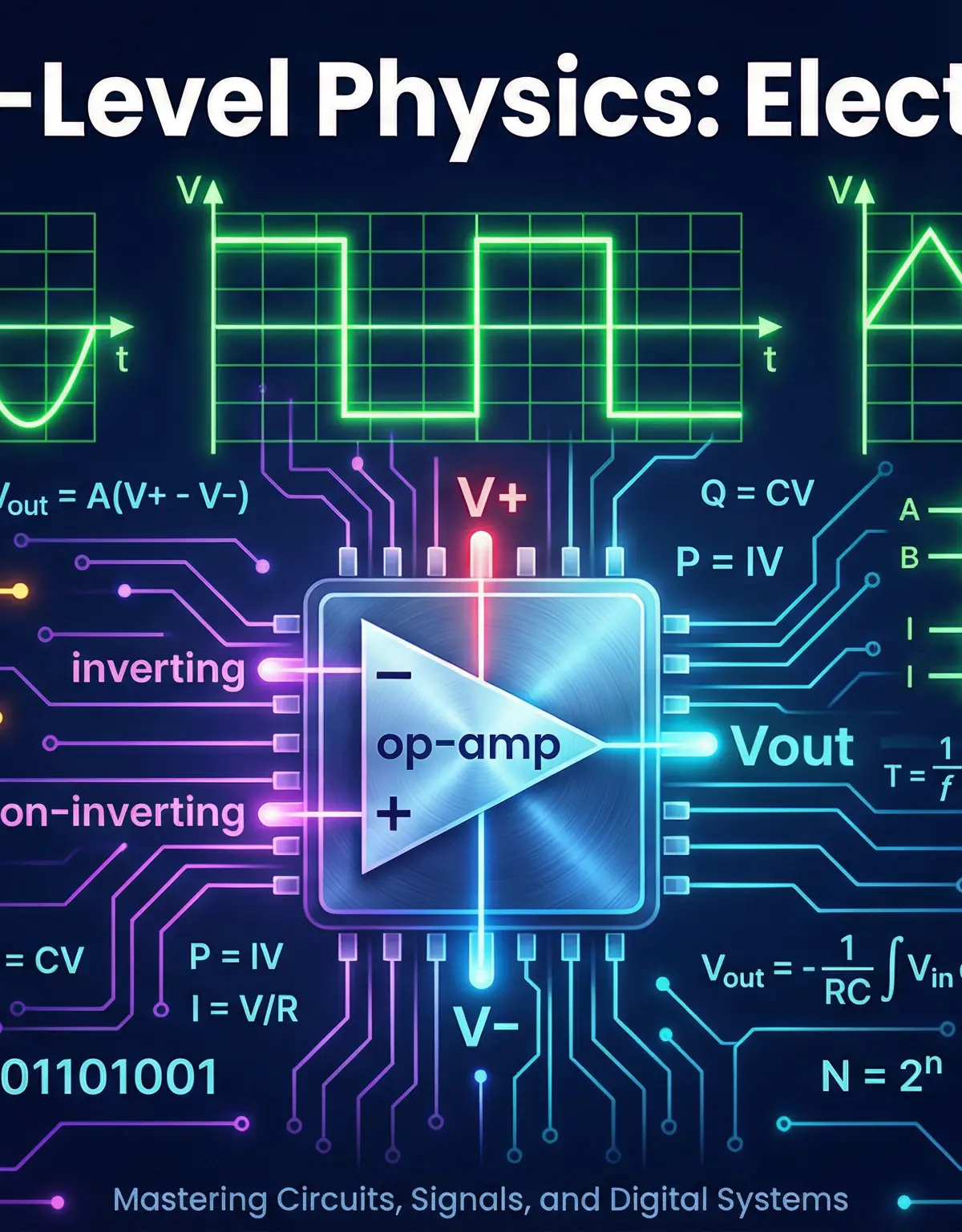
Electronics (AQA Option F, specification reference 3.9.5) is one of the most applied and intellectually satisfying options in A-Level Physics. It bridges the gap between abstract circuit theory and real engineering, requiring candidates to design, analyse, and evaluate both analogue and digital systems. The topic divides cleanly into two domains: analogue electronics, centred on the operational amplifier (op-amp) and filter circuits; and digital electronics, covering Boolean algebra, logic gate minimisation using Karnaugh maps, sequential logic, and the 555 timer.
Exam questions on this topic span all three Assessment Objectives: AO1 (knowledge recall, 30%), AO2 (application of concepts to novel circuits, 45%), and AO3 (analysis and evaluation of data or designs, 25%). The AO2 weighting is the highest, which means simply memorising formulas is insufficient — candidates must be able to apply them to unfamiliar circuit configurations. Typical question styles include multi-step gain calculations, circuit design tasks requiring specific component values, truth table completion, Boolean expression simplification, and 555 timer timing calculations.
This guide connects to related topics including capacitance (charging/discharging curves underpin the 555 timer), AC circuits (frequency response and filters), and digital communications (AM bandwidth). Synoptic questions frequently link op-amp behaviour to electromagnetic induction or sensor circuits.
Key Concepts
Concept 1: The Operational Amplifier — Ideal Properties and Open-Loop Behaviour
The operational amplifier is a high-gain differential voltage amplifier. In its ideal form, it has infinite open-loop gain (A₀ → ∞), infinite input impedance (no current flows into either input terminal), and zero output impedance (the output can drive any load without voltage drop). These ideal properties are the basis for all AQA calculations unless the question explicitly states otherwise.
The output voltage is given by: V_out = A₀(V⁺ − V⁻), where V⁺ is the non-inverting input and V⁻ is the inverting input. Because A₀ is so large (typically 10⁵ to 10⁶), even a microvolt difference between the inputs drives the output to the supply rail — this is saturation. An op-amp used without feedback (open-loop) therefore acts as a voltage comparator, not a linear amplifier.
Why does this matter for the exam? Candidates who confuse open-loop and closed-loop behaviour frequently make errors in gain calculations. The open-loop gain is the intrinsic property of the device; the closed-loop gain is set by the external feedback network and is always much smaller.
Concept 2: The Inverting Amplifier
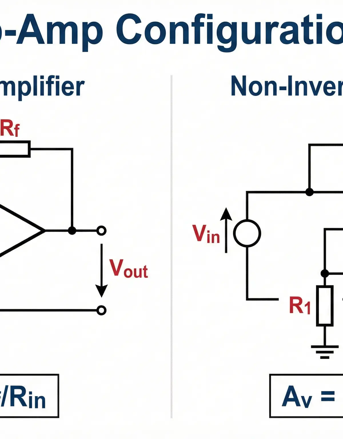
In the inverting amplifier configuration, the input signal V_in is applied through an input resistor R_in to the inverting (−) input. A feedback resistor R_f connects the output back to this same inverting input. The non-inverting (+) input is connected to ground (0 V).
Using the virtual earth approximation (which follows from the ideal op-amp's infinite gain: if V_out is finite and A₀ → ∞, then V⁺ − V⁻ → 0, so V⁻ ≈ V⁺ = 0 V), the voltage gain is:
A_v = −R_f / R_inThe negative sign is not cosmetic — it indicates a 180° phase inversion between input and output. Omitting this sign is the single most common error in this topic and costs candidates a mark every year. The magnitude of the gain is |R_f / R_in|, but the sign must be present in any answer about gain or output voltage.
Saturation check: Always calculate the theoretical output voltage (V_out = A_v × V_in) and compare it to the supply rails (±V_s). If |V_out| > V_s, the actual output is saturated at ±V_s. You must state this explicitly to receive the final mark.
Concept 3: The Non-Inverting Amplifier
In the non-inverting configuration, V_in is applied directly to the non-inverting (+) input. The feedback network (R_f from output to inverting input, R₁ from inverting input to ground) sets the gain:
A_v = 1 + R_f / R₁This gain is always ≥ 1 and there is no phase inversion. The special case where R_f = 0 and R₁ = ∞ gives A_v = 1 — this is the voltage follower (buffer), which exploits the op-amp's high input impedance and low output impedance for impedance matching.
Concept 4: Active Filters and Frequency Response
Op-amps are used to build active filters — frequency-selective circuits with gain. The cut-off (break) frequency for a simple RC filter is:
**f_c = 1 / (2πRC)**At f_c, the gain falls to 1/√2 (≈ 0.707) of its passband value, corresponding to −3 dB. A low-pass filter passes frequencies below f_c and attenuates those above; a high-pass filter does the opposite. When answering questions on filters, explicitly identify which R and C components determine the cut-off — examiners penalise vague answers that simply quote the formula without linking it to specific components.
Concept 5: Boolean Algebra and Logic Gates
Digital systems process binary signals (logic 0 = low voltage, logic 1 = high voltage). The fundamental gates are AND, OR, NOT, NAND, NOR, and XOR. Their Boolean expressions and truth tables must be memorised. NAND and NOR are universal gates — any logic function can be implemented using only NAND gates or only NOR gates, a fact that examiners test regularly.
De Morgan's Laws are the key tools for converting between implementations:
- First Law: NOT(A AND B) = NOT-A OR NOT-B → i.e., NAND(A,B) = NOT-A OR NOT-B
- Second Law: NOT(A OR B) = NOT-A AND NOT-B → i.e., NOR(A,B) = NOT-A AND NOT-B
When simplifying Boolean expressions algebraically, show each application of De Morgan's Law as a distinct intermediate step — the mark scheme awards credit for these intermediate steps.
Concept 6: Karnaugh Maps (K-Maps)
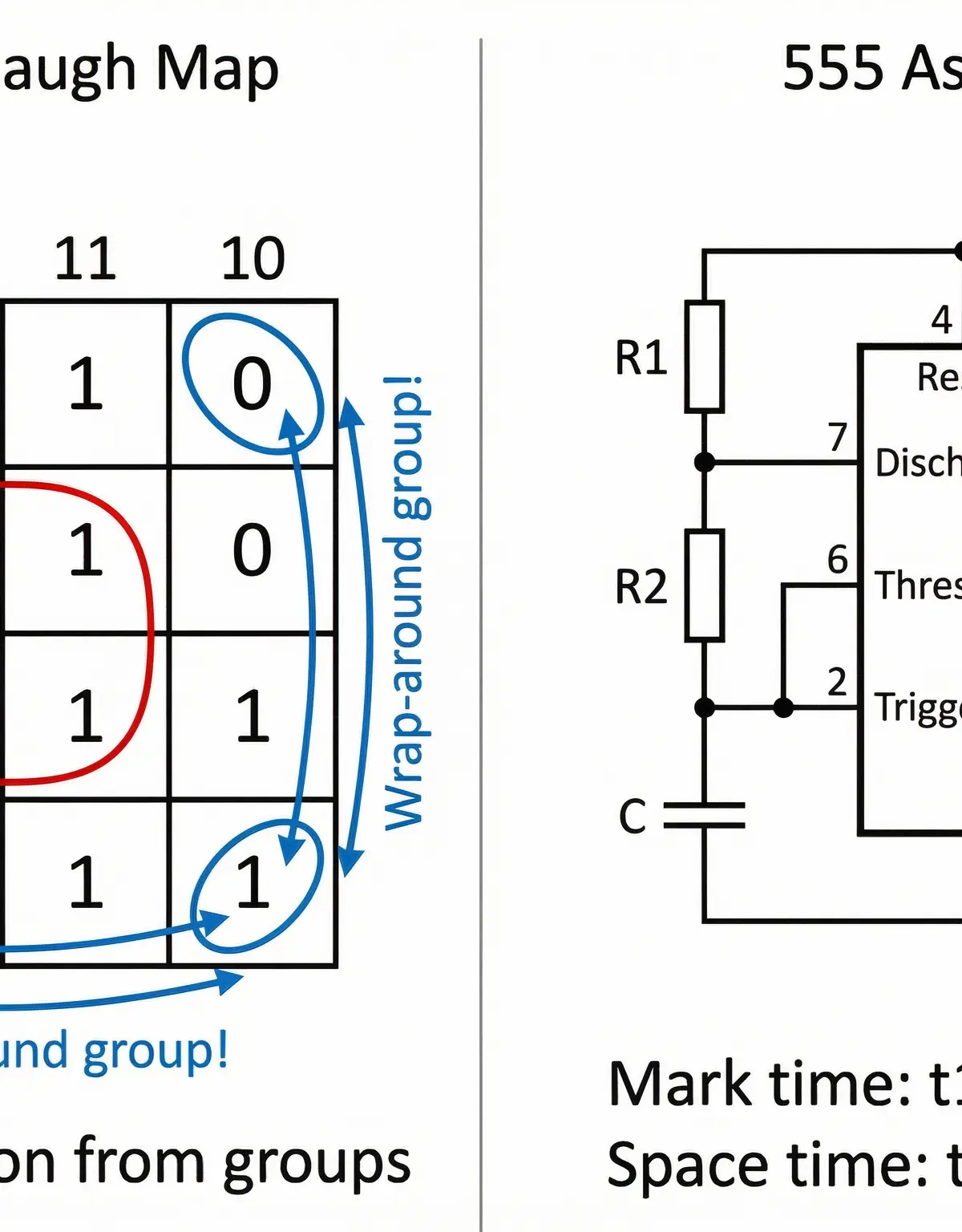
A Karnaugh map is a graphical method for minimising Boolean expressions. Cells are arranged in Gray code order (00, 01, 11, 10) so that adjacent cells differ by only one variable. The rules for grouping are:
- Group only cells containing 1s.
- Groups must be powers of 2 in size (1, 2, 4, 8, or 16).
- Make groups as large as possible — larger groups eliminate more variables.
- Groups may wrap around edges and corners of the map — this is the rule candidates most commonly miss.
- Each 1 must be covered by at least one group, but groups may overlap.
Each group of 2ⁿ cells eliminates n variables from the expression. The minimised expression is the OR of the Boolean terms from each group.
Concept 7: Sequential Logic and the D-Type Flip-Flop
Unlike combinational logic (where output depends only on current inputs), sequential logic has memory — the output depends on both current inputs and the circuit's previous state. The D-type flip-flop is the fundamental memory element: on the rising edge of a clock pulse, the output Q takes the value of the data input D, and holds it until the next clock edge. This edge-triggered behaviour is essential for synchronous digital systems such as shift registers and binary counters.
Concept 8: The 555 Timer in Astable Mode
In astable mode, the 555 timer generates a continuous square wave without any external trigger. The capacitor C charges through R₁ + R₂ and discharges through R₂ only (via the internal discharge transistor connected to pin 7). The timing formulas are:
- Mark time (output HIGH): t₁ = 0.693(R₁ + R₂)C
- Space time (output LOW): t₂ = 0.693 R₂ C
- Period: T = t₁ + t₂ = 0.693(R₁ + 2R₂)C
- Frequency: f = 1/T
The most common error is using (R₁ + R₂) for the space time. Remember: charging uses both resistors; discharging uses only R₂.
Mathematical Relationships
| Formula | Expression | Notes | Formula Sheet? |
|---|---|---|---|
| Inverting amplifier gain | A_v = −R_f / R_in | Negative sign essential | Must memorise |
| Non-inverting amplifier gain | A_v = 1 + R_f / R₁ | Always ≥ 1, no inversion | Must memorise |
| Op-amp output voltage | V_out = A_v × V_in | Check against ±V_s | Must memorise |
| Cut-off frequency | f_c = 1 / (2πRC) | −3 dB point | Must memorise |
| 555 mark time | t₁ = 0.693(R₁ + R₂)C | Charging path | Must memorise |
| 555 space time | t₂ = 0.693 R₂ C | Discharging path | Must memorise |
| 555 frequency | f = 1 / [0.693(R₁ + 2R₂)C] | Derived from T = t₁ + t₂ | Must memorise |
| AM signal bandwidth | BW = 2f_m | f_m = highest modulating freq | Must memorise |
Practical Applications
Op-amps appear in audio amplifiers, instrumentation amplifiers (measuring small sensor signals), and active crossover filters in speaker systems. The 555 timer is found in everything from LED flashers to pulse-width modulation motor controllers. Digital logic underpins all computing hardware, from simple combinational circuits to complex sequential processors. Understanding these applications helps contextualise exam questions that present novel circuit configurations — the underlying physics is always the same.
Visual Resources
2 diagrams and illustrations


Interactive Diagrams
3 interactive diagrams to visualise key concepts
Conceptual Flow Outline
Decision flowchart for identifying op-amp configuration and applying the correct gain formula, including the mandatory saturation check.
Conceptual Flow Outline
Step-by-step process for completing a Karnaugh map minimisation, highlighting the wrap-around group check that candidates most commonly miss.
Conceptual Flow Outline
Simplified 555 astable timer signal flow showing the charging path (through R1 + R2, shown in red/blue) and the discharging path (through R2 only, shown in blue). This distinction is the source of the most common timing calculation error.
Worked Examples
4 worked examples — open one to explore the question and available guidance.
Practice Questions
Try the question, then reveal an answer plan or example response
State the two properties of an ideal operational amplifier that are used to derive the inverting amplifier gain formula A_v = −R_f/R_in. [2 marks]
Hint: Think about what happens to the current into the op-amp inputs, and what happens to the voltage difference between the two inputs when negative feedback is applied.
A non-inverting amplifier is required to have a voltage gain of 15. The feedback resistor R_f = 56 kΩ. Calculate the value of R₁ required. [3 marks]
Hint: Write the non-inverting gain formula, substitute A_v = 15 and R_f = 56 kΩ, then rearrange for R₁.
A 555 timer in astable mode uses R₁ = 10 kΩ, R₂ = 22 kΩ, and C = 47 nF. (a) Calculate the frequency of the output waveform. (b) Calculate the duty cycle (mark time as a percentage of the total period). [5 marks]
Hint: Calculate t₁ and t₂ separately using the correct formulas, then find T = t₁ + t₂ for frequency. Duty cycle = t₁/T × 100%.
A logic system has three inputs A, B, and C. The output F is HIGH only when an odd number of inputs are HIGH. Complete the truth table and write the Boolean expression for F. Hence implement F using only NAND gates. [6 marks]
Hint: An odd number of HIGH inputs means either exactly 1 or exactly 3 inputs are HIGH. The Boolean expression for this is the XOR function extended to three variables: F = A ⊕ B ⊕ C. For the NAND implementation, use De Morgan's Laws to convert each gate.
An active low-pass filter has a passband gain of 20 dB and a cut-off frequency of 2.0 kHz. The capacitor used is 10 nF. Calculate (i) the passband voltage gain, (ii) the value of the resistor R that sets the cut-off frequency. [4 marks]
Hint: Convert dB gain to voltage gain using A_v = 10^(dB/20). Then use f_c = 1/(2πRC) rearranged for R.
Exam technique
How to turn what you know into marks
How to approach the question
Read the full question before writing anything. Identify: (1) which circuit configuration is shown (inverting/non-inverting/555/filter); (2) which formula is needed; (3) whether a saturation check is required; (4) whether the question asks for NAND-only or NOR-only implementation. Annotate the circuit diagram with known values before starting calculations.
How to structure your answer
For 1–2 mark questions: state the answer with correct units and sign. For 3–4 mark calculations: write the formula first, substitute values with units, calculate, then perform the saturation check. For 5–6 mark design/explain questions: structure as (i) state the principle, (ii) apply to the specific circuit, (iii) draw a conclusion or evaluate. For K-map questions: always draw the map, show all groupings with loops, then write the expression.
Timing
Approximately 1 minute per mark at A-Level. A 6-mark question should take 6–7 minutes including checking. Electronics questions often involve multi-step calculations — allocate an extra 30 seconds for the saturation check on any op-amp question.
Common pitfalls
- Omitting the negative sign in inverting amplifier gain — A_v = −R_f/R_in, not +R_f/R_in. The negative sign indicates phase inversion and is a distinct marking point. Fix: always write the formula with the minus sign before substituting.
- Using (R₁ + R₂) for the 555 space time instead of R₂ alone — the capacitor discharges only through R₂ because pin 7 (discharge) bypasses R₁. Fix: draw the charging and discharging paths on the circuit before writing the formulas.
- Using binary column order (00, 01, 10, 11) instead of Gray code (00, 01, 11, 10) in K-maps — this breaks the adjacency property and produces wrong groupings. Fix: write 'Gray code: 00, 01, 11, 10' at the top of every K-map as a reminder.
- Missing wrap-around groups in K-maps — the four corner cells of a 4-variable map can form a valid group of four. Fix: after identifying all obvious groups, systematically check all four edges and all four corners.
- Stating the bandwidth of an AM signal as the carrier frequency rather than twice the highest modulating frequency. Fix: BW = 2f_m — the carrier frequency is irrelevant to bandwidth.
What the command words want
- Compare
- Identify both similarities AND differences using comparative language ('whereas', 'in contrast', 'both'). For comparing inverting and non-inverting: address gain formula, phase relationship, and input impedance.
- Explain
- Say HOW or WHY using 'because' to link cause and effect. For op-amp saturation: 'The output saturates at +9 V because the theoretical output of +12 V exceeds the positive supply rail.'
- Describe
- Say what happens or what the circuit does — use correct technical terminology. For waveforms, describe amplitude, frequency, and phase relative to input.
- Evaluate
- Consider both sides of an argument, use quantitative evidence where possible, and make a clear judgement. For circuit design evaluation: assess whether the design meets the specification and identify any limitations.
- Calculate
- Show the formula first, substitute values with units, calculate step by step, state the final answer with units. Always perform the saturation check for op-amp output calculations.
- State/Give
- Brief factual answer — 1–2 words or a short phrase. No explanation needed. Example: 'State the voltage gain' → write the formula or numerical value only.
Watch or listen (optional)
Test your understanding of Electronics
Active recall beats re-reading. Take an instant quiz now to test what you’ve learned and lock it into long-term memory.
A week of Premium from your first lesson · Then the free plan continues · No card, no charge