Pearson Edexcel · GCSE · Design and Technology
Systems: Alternative processes that can be used to manufacture components and systems to different scales of production
This topic covers the essential manufacturing processes for electronic systems, from photo etching custom PCBs to understanding the leap from breadboard prototyping to automated mass production. Mastering this area is crucial for evaluating how scale and technology dictate the way electronic products are made in the real world.
- 7 min read
- 3 worked examples
- 3 practice questions
- 6 key terms
Study Notes
Overview
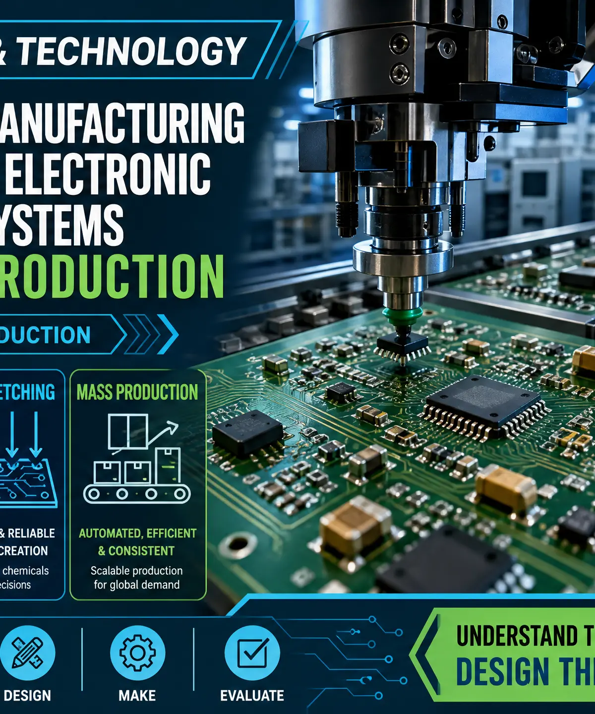
In Design and Technology, understanding Systems is about more than just knowing what a resistor or capacitor does. It's about understanding how these components are assembled into functional products at different scales. Topic 5.6 focuses on the alternative processes used to manufacture components and systems, specifically focusing on Printed Circuit Boards (PCBs) and how the scale of production dictates the manufacturing methods chosen.
Key Knowledge & Theory
Core Concepts
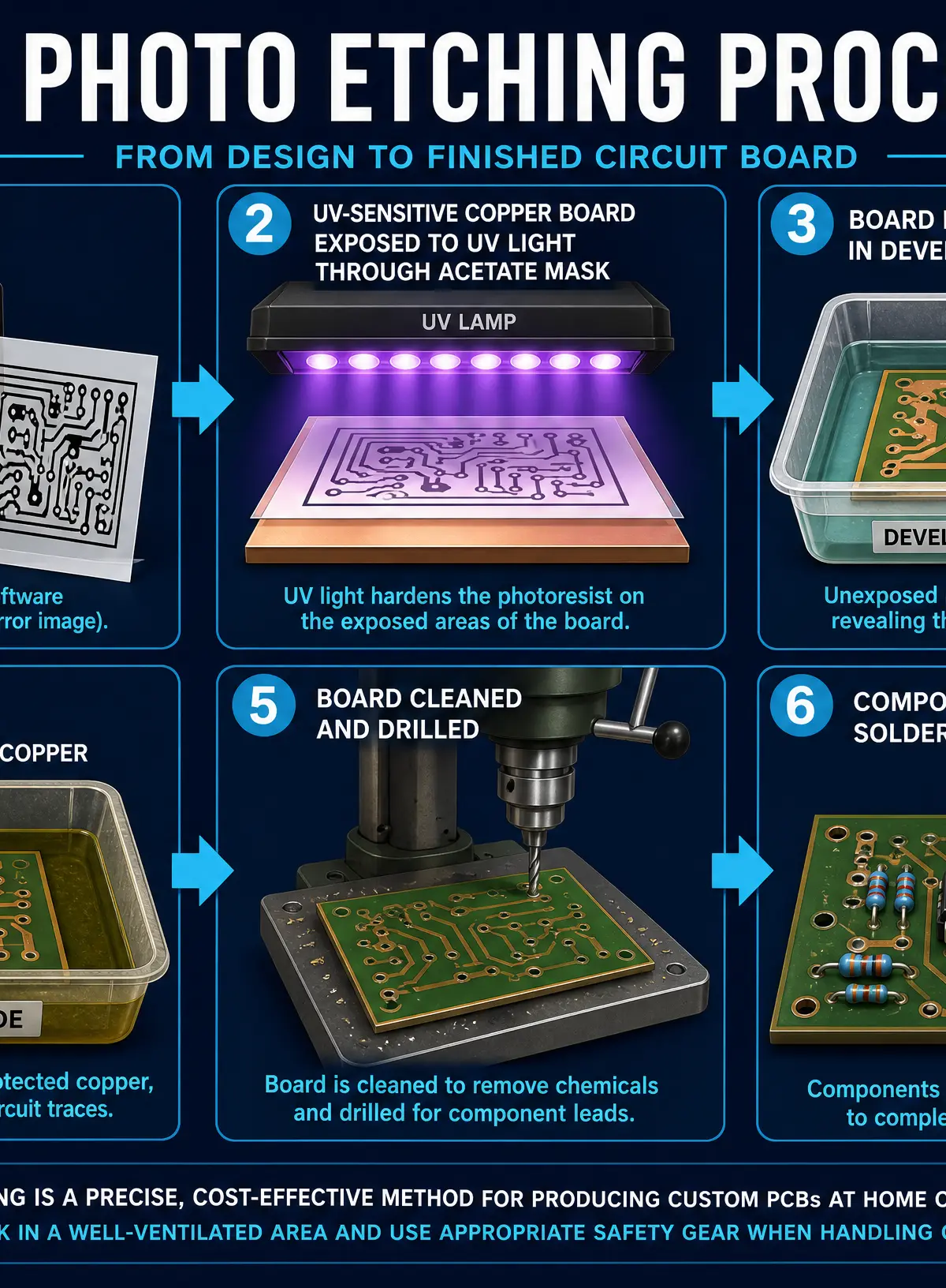
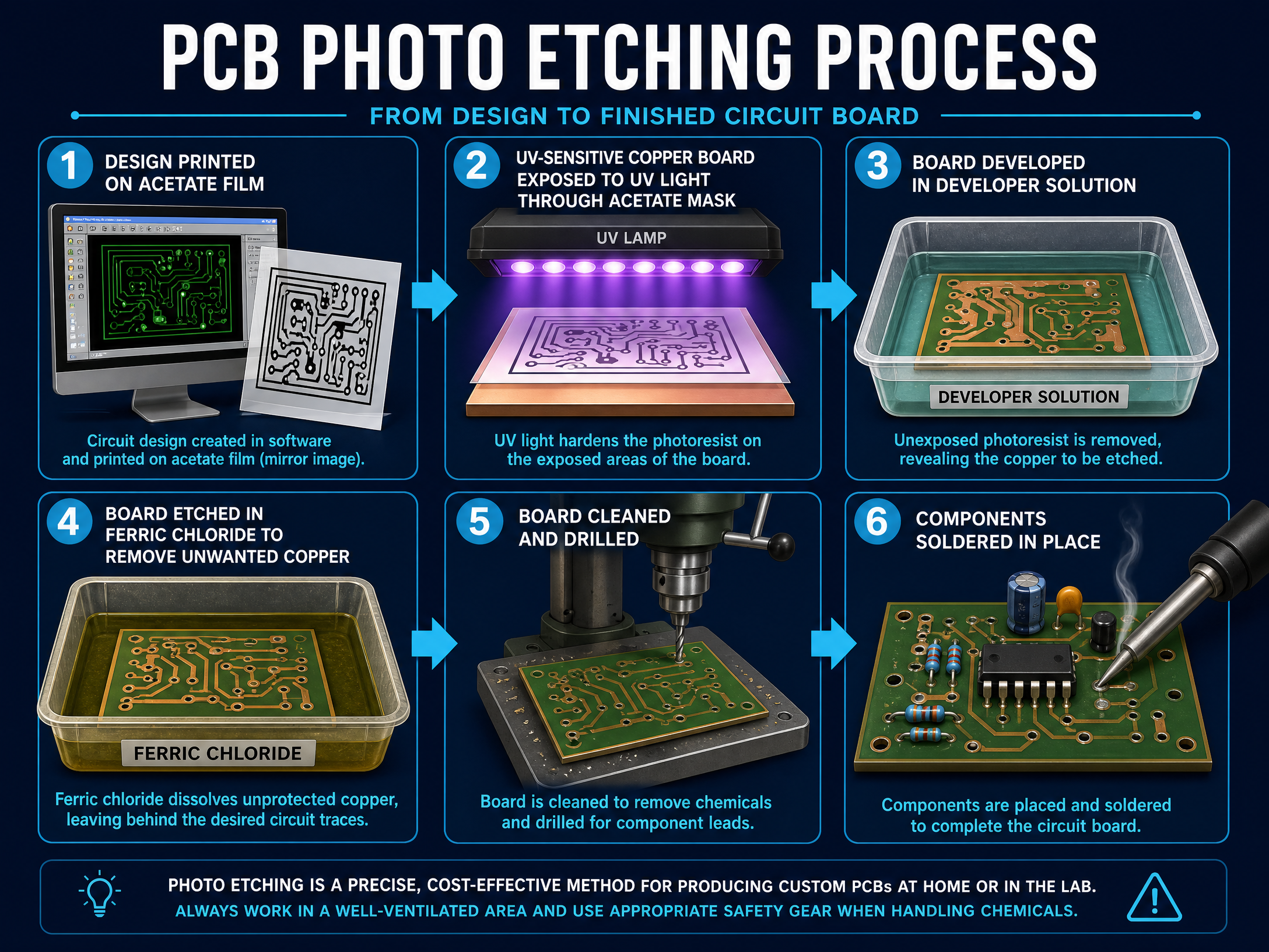
1. Printed Circuit Board (PCB) Manufacturing: Photo EtchingPhoto etching is the standard process for producing custom PCBs. It uses light and chemicals to create precise copper tracks that connect electronic components. The process follows a strict sequence:
- Design: The circuit layout is created using CAD software and printed onto a transparent acetate film (the mask).
- Exposure: A copper-clad board coated with light-sensitive photoresist is placed under the mask and exposed to UV light. The light hardens the exposed areas.
- Development: A developer solution washes away the unexposed, soft photoresist.
- Etching: The board is submerged in ferric chloride, which dissolves the unprotected copper, leaving only the desired circuit tracks.
- Finishing: The board is cleaned, and holes are drilled for component leads.
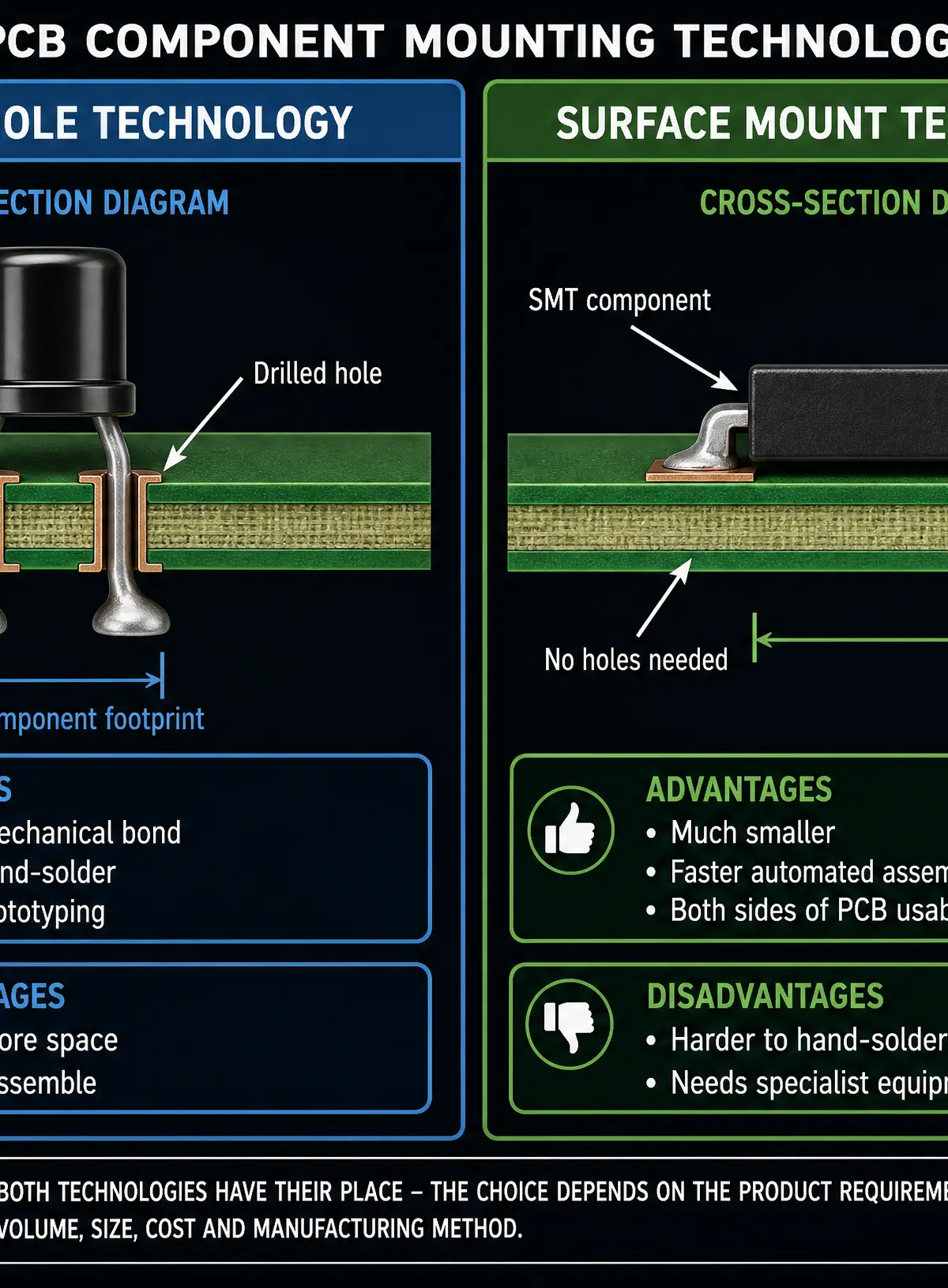
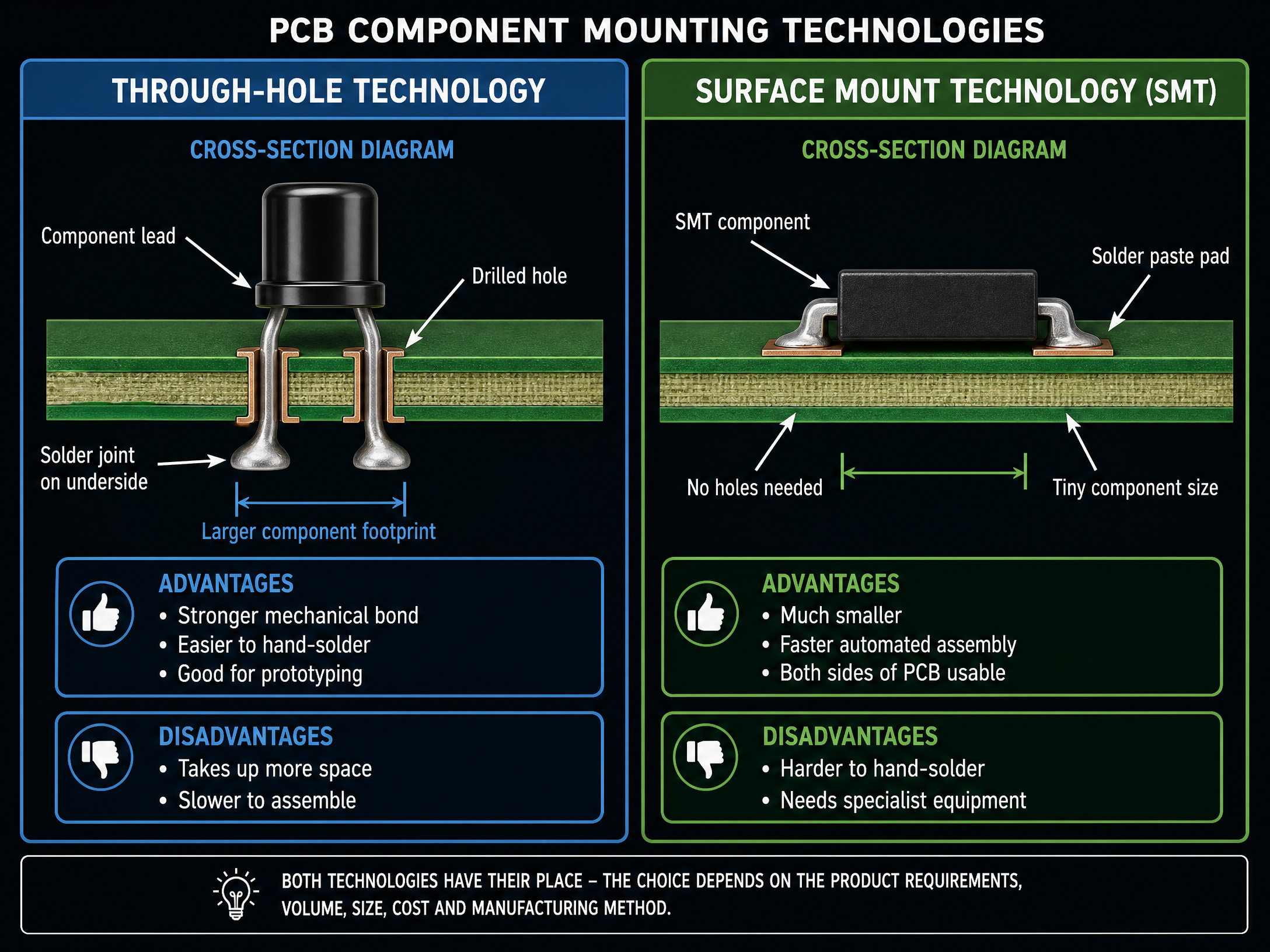
2. Component Mounting TechnologiesThere are two primary ways to attach components to a PCB:
- Through-Hole Technology: Component leads are pushed through drilled holes in the PCB and soldered on the underside. This creates a strong mechanical bond and is ideal for prototyping or components that will undergo physical stress, but it takes up more space and requires drilling.
- Surface Mount Technology (SMT): Tiny components are soldered directly onto pads on the surface of the PCB. No holes are needed. This allows for much smaller devices, double-sided board population, and rapid automated assembly using pick-and-place machines.
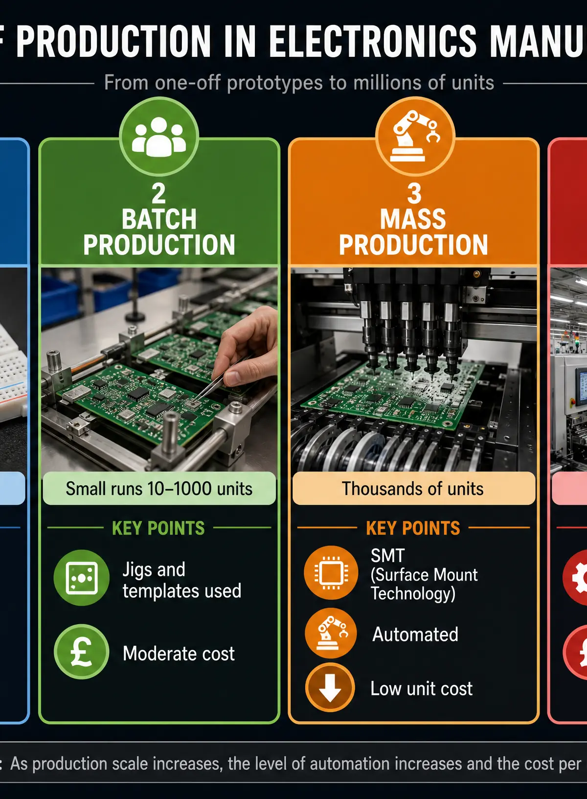
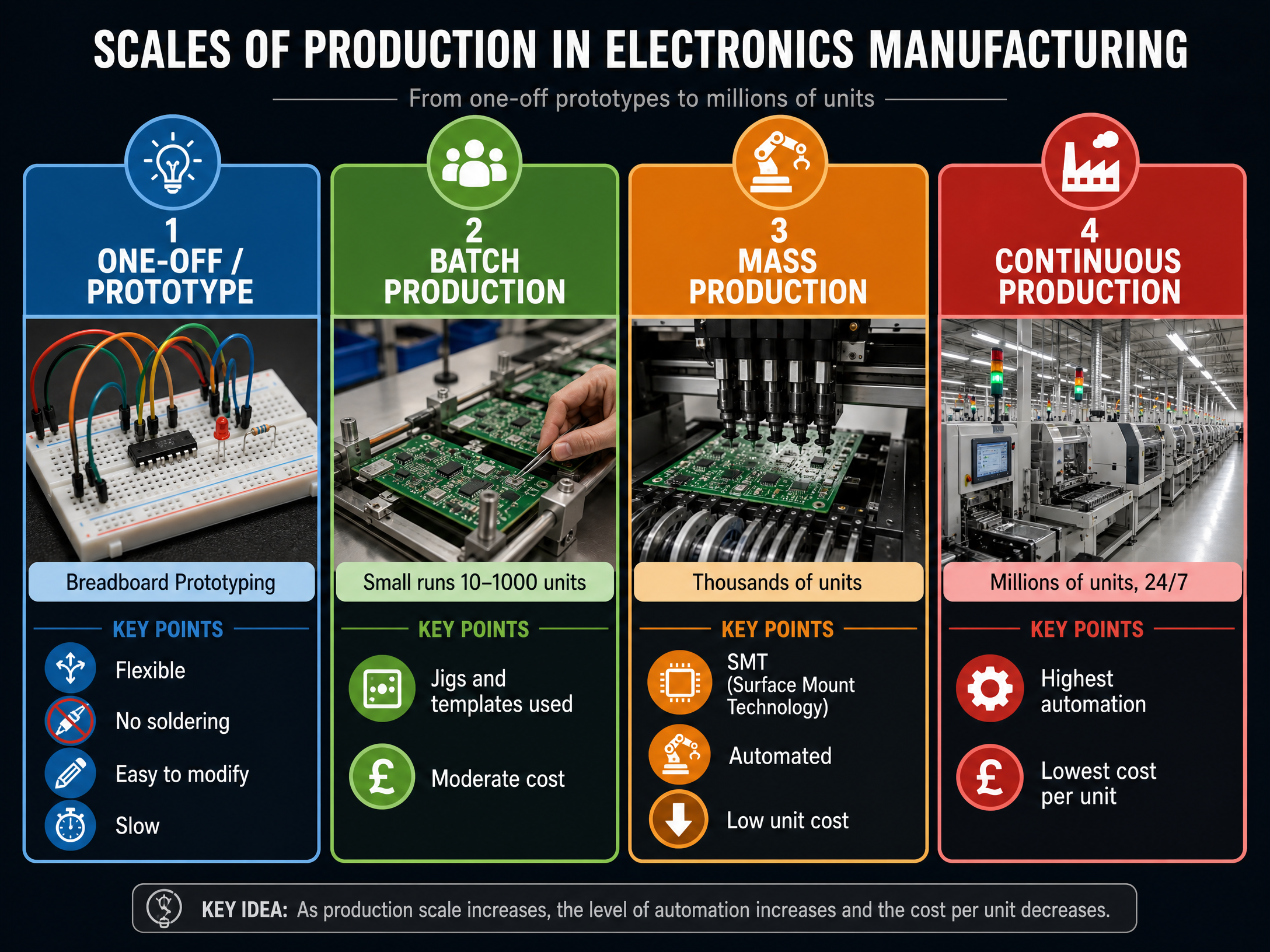
3. Scales of ProductionThe scale of production dictates the manufacturing methods, tools, and level of automation used.
- One-off / Prototyping: Making a single product to test a concept. In electronics, this usually involves a breadboard, allowing components to be connected without soldering for easy modification.
- Batch Production: Producing a set quantity (e.g., 100 units). Uses jigs (to hold workpieces) and templates (for marking out) to ensure consistency across the batch without the massive setup costs of full automation.
- Mass Production: Producing thousands of identical products. Relies heavily on automation, specifically SMT and pick-and-place machines, to achieve high speed and low unit costs.
- Continuous Production: 24/7 manufacturing of millions of units (e.g., standard resistors or microchips). Requires massive initial investment but delivers the absolute lowest cost per unit.
Technical Vocabulary
- Photoresist: A light-sensitive polymer applied to copper-clad boards before UV exposure.
- Ferric Chloride: The chemical etchant used to dissolve unprotected copper.
- Pick-and-Place Machine: A robotic system used in mass production to rapidly place SMT components onto a PCB.
- Reflow Soldering: A process where solder paste is melted in an oven to permanently attach SMT components.
- Tolerance: The acceptable margin of error in a measurement or dimension.
- Jig: A custom-made tool used to control the location and motion of another tool, or to hold a workpiece securely.
Practical Skills
Techniques & Processes
When undertaking practical systems work for your NEA (coursework), you must demonstrate safe and accurate manufacturing skills.
Soldering Best Practice
- Ensure the soldering iron tip is clean and 'tinned' (coated with a thin layer of solder).
- Heat the component lead and the copper pad simultaneously for 2-3 seconds.
- Apply a small amount of solder to the joint, not directly to the iron.
- Allow the joint to cool naturally without blowing on it to avoid a 'cold joint' (which looks dull and may fail).
**Quality Control (QC)**In practical work, QC means checking your work against the specification. In industry, it involves:
- Visual Inspection: Manually checking for solder bridges or missing components.
- Automated Optical Inspection (AOI): Using cameras and software to rapidly inspect mass-produced boards.
- Electrical Testing: Using a multimeter to check for continuity (no breaks in tracks) and shorts (unintended connections).
Portfolio/Coursework Guidance
Assessment Criteria
Examiners award marks in the NEA for demonstrating a logical, iterative design process. For systems projects, this means:
- AO1 (Identify and Investigate): Researching existing electronic products and component specifications.
- AO2 (Design and Make): Evidencing breadboard prototyping, circuit simulation (e.g., using Yenka or Circuit Wizard), and high-quality PCB manufacture.
- AO3 (Analyse and Evaluate): Testing the final circuit against the initial specification and suggesting improvements.
Building a Strong Portfolio
To secure top marks, document your prototyping phase thoroughly. Don't just show the final working circuit. Include photographs of your breadboard tests. If a circuit didn't work initially, explain why and show how you fixed it. This demonstrates deep understanding and problem-solving skills, which examiners highly reward.
Exam Component
Written Exam Knowledge
The written paper will frequently test your ability to select appropriate manufacturing methods for different scenarios. You must be able to justify why a particular scale of production or component type is suitable.
Listen to our revision podcast for a full walkthrough of how to approach these questions:

Exam Strategy: The 'Evaluate' Question
Questions asking you to evaluate manufacturing processes (e.g., "Evaluate the use of SMT for manufacturing a mobile phone motherboard") are usually worth 6-8 marks. You must:
- State the advantages (e.g., smaller size, faster automated assembly).
- State the disadvantages (e.g., high initial setup cost for machinery, difficult to repair manually).
- Provide a justified conclusion linking back to the product (e.g., because mobile phones are mass-produced in the millions, the high setup costs are justified by the low unit cost and the necessity for miniaturisation).
Visual Resources
3 diagrams and illustrations
Interactive Diagrams
1 interactive diagram to visualise key concepts
Conceptual Flow Outline
Decision matrix for selecting scales of production in electronics manufacturing.
Worked Examples
3 worked examples — open one to explore the question and available guidance.
Practice Questions
Test your understanding — click to reveal model answers
State the name of the chemical used to remove unwanted copper during PCB manufacture. [1 mark]
Hint: It contains iron and chlorine.
Explain one advantage of using a breadboard when developing a new electronic circuit. [2 marks]
Hint: Think about what happens if you make a mistake.
A company is designing a new smartwatch. Discuss the manufacturing processes and technologies they should use for the internal circuitry. [6 marks]
Hint: Consider the scale of production for a smartwatch and the space constraints inside the casing.